Tuesday, 28.03.2017
This is not a love song... After doing a lot of PCB's the last couple of weeks with the toner transfer method, I thought about a faster and more reliable method to transfer my layout. Basically the toner transfer method works fine, but it is too time consuming and not reliable enough. (new paper, new printer and everything is turned upside down...) Straight ahead, I started with designing an UV-LED MATRIX with 84 LED...
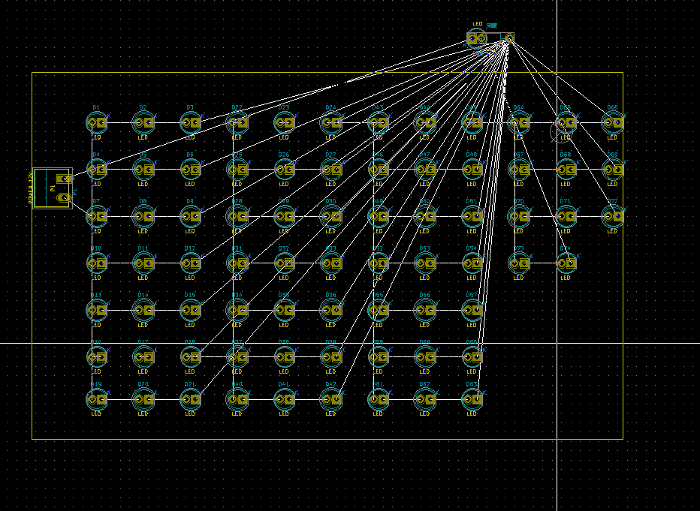
Routing- in this case a repetive work
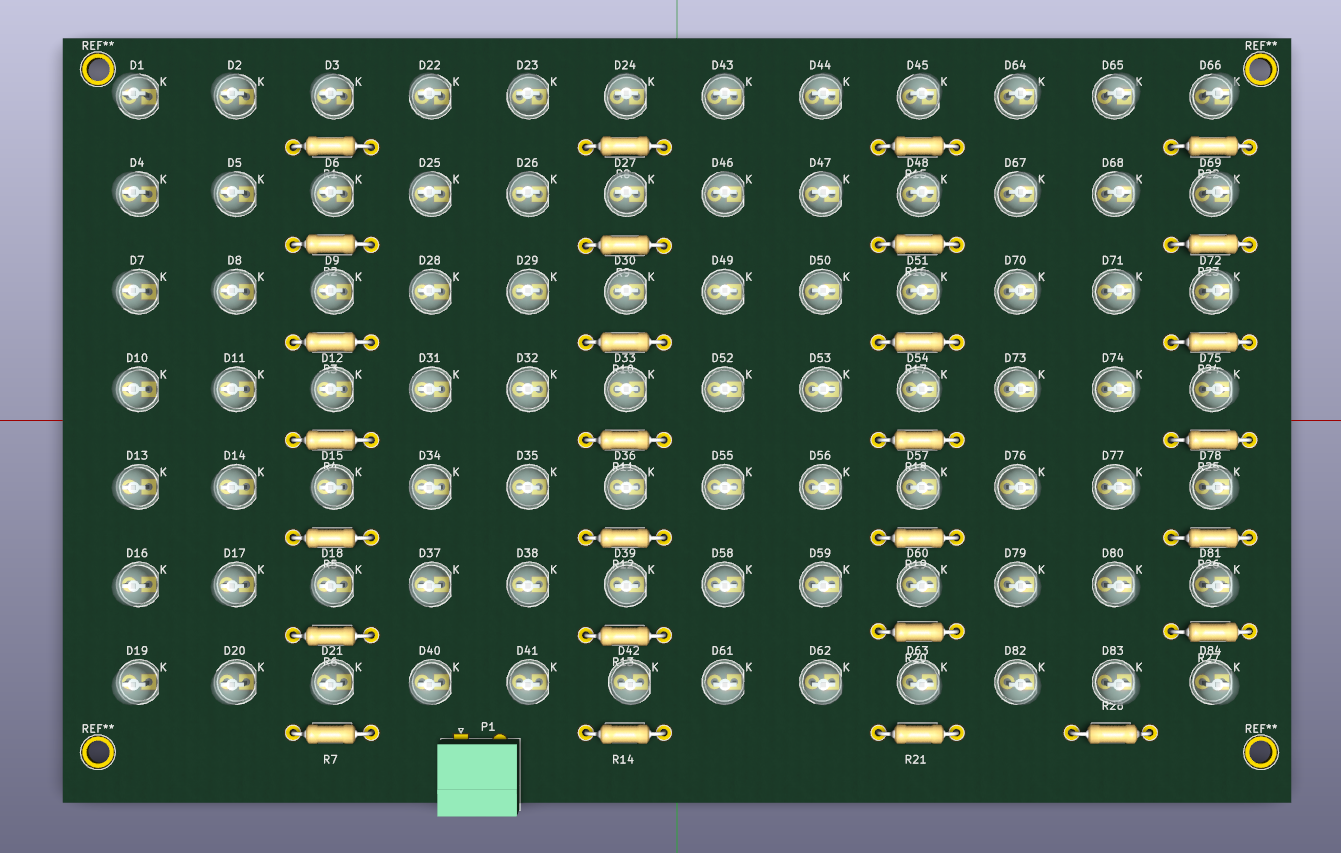
The PCB 160mm*100mm
| PART | VALUE | AMOUNT |
|---|---|---|
| LEDS UV | 3.3V/20mA | 84 |
| R | 120 Ohm | 28 |
| Screw terminal block | 2Pole,5mm | 1 |
I hope that was the last one I did with the toner transfer method...
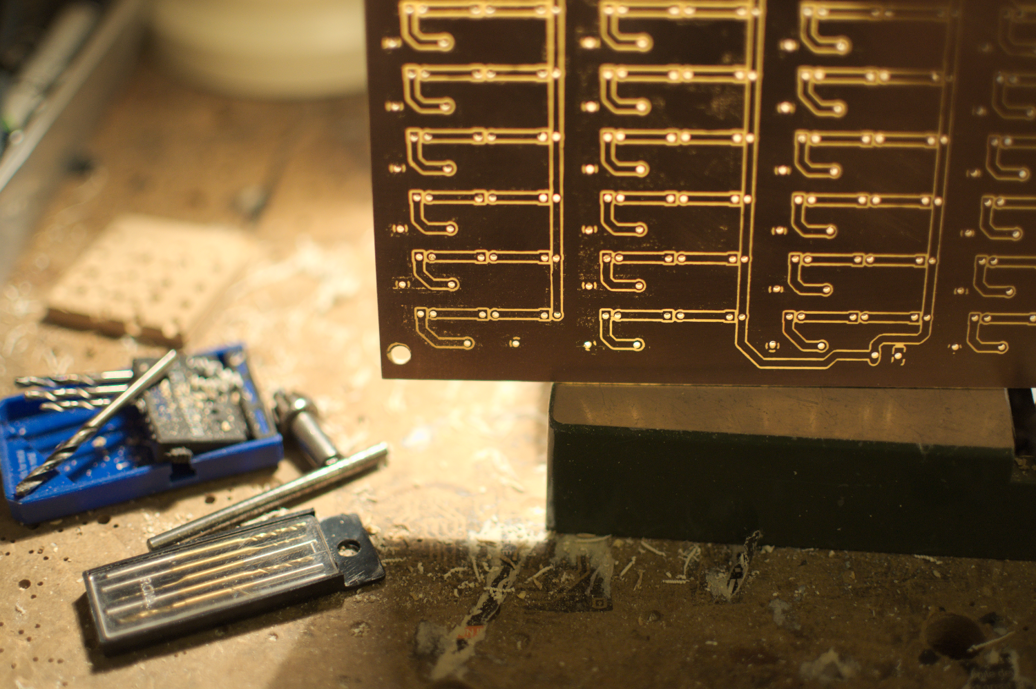
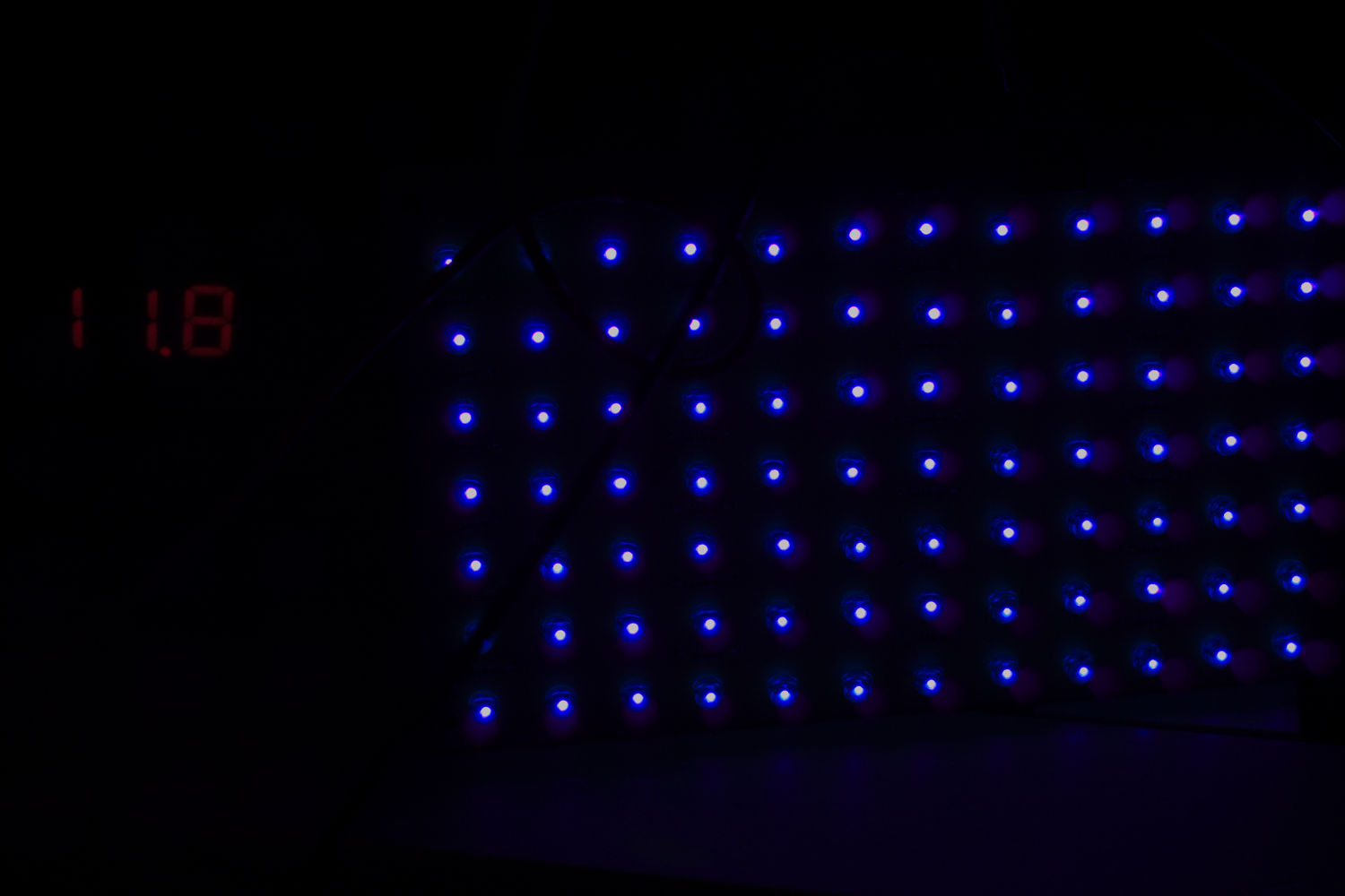
The PCB turned out quite well. You can see small interferences on the ground plate. I guess they come from my (formerly broken 25 €) black and white laser printer. The drilling and soldering work took me some time and after hooking it up I had just one faulty LED and two tracks I routed false in a hurry...
Download the KICAD project files for the UV-LED-Matrix. I used Kicad 4.0.5. I correced my routing mistake.
13.04.2017
Just a short update to myself: I already did a few pcb's with my exposurebox. For now it is just an old shoebox and a "milky acrylic glass"... I get the best results with an exposure time between 3 and 3:30 minutes. (with the expensive photoPCB's ;-)) Only (minor) problem is my laser printer, which prints just awful! So I use some "toner compactor" to get a more dense printing picture.